I have been curious about digital electronics for a long time and have attempted to learn the subject making significant progress when I watched Building an 8-bit breadboard computer! by Ben Eater on YouTube quite a long time ago. I also partially read Digital Computer Electronics - Malvino, Paul. However, I never got myself to gather the components to actually build a ‘breadboard’ computer myself. Being a person who learns by doing and not just watching, this left me without a true grasp of fundamental concepts of digital electronics.
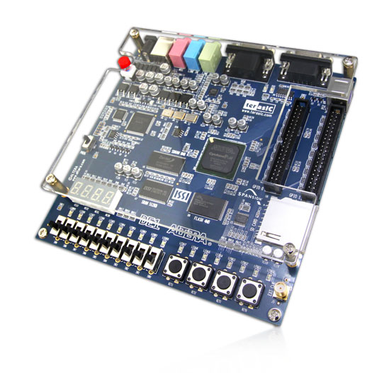
I knew something called FPGAs and CPLDs existed since working on an advanced DVB settop box around 2005 where it was innovatively used to communicate between two processors. However, I was never truly curious about it thinking that it was part of some dark art that needed brilliant brains to comprehend. Until, a few months ago (November 2025), by chance, I stumbled upon the most beautiful looking educational board on FB Marketplace called “Altera DE1” which the owner parted with for A$35.
When I switched it on, it ran the factory demo with running lights and cyclic hex numbers on the seven-segment displays. After researching a little, I realized that it was a phased-out board but had immense educational value with the ability to host a RISC soft-core processor called Nios II. The amount of ‘hardware’ that could be crammed into this board opened a plethora of possibilities in my mind. It was a mysterious concoction that sparked immense cuirosity and triggered quite a compulsion to get something useful working on the board.
I downloaded “Quartus II v13.1” which was releaed on 2013 and set about making it work on a modern Linux Mint machine. Surprisingly, with slight tweaks by zkrx, it now runs like a charm crunching away synthesis, analysis, fitting etc. required to compile VHDL code into something that can be loaded onto the FPGA and turn the board into whatever custom machine one can imageine. Of course, you can get an upgraded FPGA which would also most probably have a hard-processing system which you can communicate with the FPGA part of the machine. However, the DE1 is sufficient for my current needs so I don’t see the point of a ugrading yet.
As part of my personal tradition, historically whenever I learnt a new interactive language or framework like VisualBasic (1992) or C(1993) or HTML/JavaScript (2001) or QT (2005) or Arduino(2016), or any other, I would always make a calculator as my first project. So it made absolute sense to make one as the first major project when learning the closest to pure hardware with a board that has facinating I/Os.
Starting with knowing absolutely nothing about FPGAs, in about a months time, working a few hours every week, I was able to grasp the very basics and make a small 3 decimal digit 2-s compliment integer calculator that demonstrates some of the fundamental concepts I encountered. It may not look like much but it got me ready for the next step which will be an 8-digit fixed-point calculator which I hope to soon publish. In the meanwhile, if you are an absolute beginner like me, I invite you to follow along the journey of 10 short lessons with the hope that it may spark your curiosity too.
I have used LLMs extremely sparingly in this project as I believe that AI is a surefire way to loose all joy in learning. I have published the source code of this journey on GitHub in a public repository called fareed1983/fpga-zero-to-calculator.
A field-programmable-gate-array (FPGA) is an integrated circuit containing a grid array of programmable logic cells that can be configured in different ways and interconnected to mimic digital logic devices. Individually, each cell can be configured to act as simple logic gates and perform complex combinational and sequential functions as configured units. There are specialized languages used to configure FPGAs out of which, this tutorial uses Verilog. These custom hardware devices could be as simple as a push-button turning on an LED to as complex as and advanced system-on-chip.
The first ‘program’ I tried was an example provided in Embedded SoPC Design with Nios II Processor and Verilog Examples (Pong P. Chu, 2012) discussed in Chapter 2 with a short tutorial in section 3.5. It describes a a gate-level combinational circuit using the hardware description language (HDL) called Verilog. The code listing is available at - https://github.com/fareed1983/fpga-zero-to-calculator/tree/main/00-comparator. The first two switches of the DE1 (SW0 & SW1) are compared with the next two switches (SW2 & SW3) and if they are equal an LED lights up. It was simple but powerful to get a hang on how to use Quartus II and Verilog HDL. Detailed instructions are provided in the book to get this program up and running. On a high-level these instructions include: *
The file list_ch03_01_eq1.v implements a gate-level 1-bit comparator. When compiled, Quartus II compiles the project performing elaboration, systhesis, placement and routing into the FPGA ultimately mimicing how such a circuit would be created using logic-gates. The following ‘netlist’ is synthesized from the code.
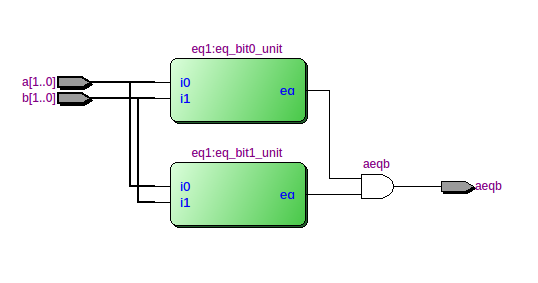
The diagram is produced by the Quartus II Netlist Viewer and shows the 2-bit comparator composed of 2 units of 1-bit comparitors. The inputs of the comparators are SW0 to SW3. These keys are mapped using the eq2.pin.csv file. The output of the comparators is then ANDed to give the result which is connected to LED0. Zoomming into one of the 1-bit comparators, we see the following gate-level diagram.
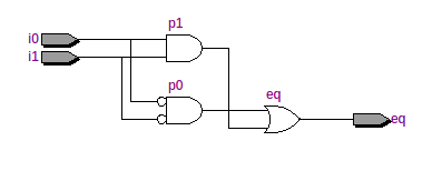
The diagram above zooms into one of the coparitor blocks in green in the first diagram. It shows a very basic 1-bit comparator and is quite self-explanatory. One point to note is that the ‘code’ in a HDL here is combinatorial logic and produces a circuit all-at-once unlike instructions provided to a microprocessor. We are building custom special-purpose machines rather than programming a general-purpose computer.
I moved on to Malvino’s Digital Computer Electronics with the aim of making the described computer using gate-level logic to get a deep grasp of the topic. However, that’s not what I found out later and thus switched strategy later.
I started this monumental task with rereading parts of the brilliant book and made the simplest adder at the gate-level in Verilog HDL.
The file listing of ha.v is as follows:
module ha
    (
        input wire a, b,
        output wire c, s
    );

    assign c = a & b;
    assign s = a ^ b;

endmodule
The above describes a half-adder module with inputs, a & b and outputs c & s. The assign statements lead to LUTs on the FPGA being configured to mimic gates. It synthesizes a combinational half-adder circuit with the following truth-table:
| a | b | sum | carry |
|---|---|---|---|
| 0 | 0 | 0 | 0 |
| 0 | 1 | 1 | 0 |
| 1 | 1 | 0 | 1 |
The other file tst.v is a simple rig connecting switches (SW) and red-LEDs (LEDR) on the board. The pin-assignments to use by default is provided in the root folder.
Next, I implemented a full-adder with the following truth table:
| a | b | carry_in | sum | carry_out |
|---|---|---|---|---|
| 0 | 0 | 0 | 0 | 0 |
| 0 | 1 | 0 | 1 | 0 |
| 1 | 1 | 0 | 0 | 1 |
| 0 | 0 | 1 | 1 | 0 |
| 1 | 0 | 1 | 0 | 1 |
| 1 | 1 | 1 | 1 | 1 |
Full adders can be chained and the carry output of the previous can be provided as carry input thus creating an adder of multiple bits.
Here, I used the previously created full-adder to chain them to add two 4-bit numbers inputted from SW0-SW3 & SW5-SW8. The output is provided in 5 bits on the green LEDs from LEDG[0]-LEDG[4]. Following is the code listing of the top-level module in the file ba.v:
module ba
    (
        input wire[0:8] SW,
        output wire[0:4] LEDG
    );

    wire [0:3] carry;

    ha ha0 (.a(SW[0]), .b(SW[5]), .sum(LEDG[0]), .carry(carry[0]));
    fa fa1 (.a(SW[1]), .b(SW[6]), .c(carry[0]), .sum(LEDG[1]), .carry(carry[1]));
    fa fa2 (.a(SW[2]), .b(SW[7]), .c(carry[1]), .sum(LEDG[2]), .carry(carry[2]));
    fa fa3 (.a(SW[3]), .b(SW[8]), .c(carry[2]), .sum(LEDG[3]), .carry(LEDG[4]));

endmodule
The above synthezises into a circuit resembling the diagram below from Wikipedia except that the first block is a half-adder as there is no requirement for a carry-in.

The following video from Ben Eater provides an excellent explanation of how this works:
Next I moved on to revising how 2-s compliment works and making a 2-s compliment adder and subtractor circuit. This project gave me a good grasp of 2-s compliment denomination which I had learnt many times in C-programming books but never fully comprehended before. It is easy to understand from the HDL code listing of as2c.v below and compare it to Malvino’s Fig. 6-7.
module as2c
    (
        input wire[3:0] a, b,
        input wire sub,
        output wire [3:0] sum,
        output wire overflow
    );

    wire [3:0] c;
    wire[3:0] bn;
    assign bn = b ^ {4{sub}};

    fa fa0 (.a(a[0]), .b(bn[0]), .c(sub),   .sum(sum[0]), .carry(c[0]));
    fa fa1 (.a(a[1]), .b(bn[1]), .c(c[0]),  .sum(sum[1]), .carry(c[1]));
    fa fa2 (.a(a[2]), .b(bn[2]), .c(c[1]),  .sumf(sum[2]), .carry(c[2]));
    fa fa3 (.a(a[3]), .b(bn[3]), .c(c[2]),  .sum(sum[3]), .carry(c[3]));

    assign overflow = c[2] ^ c[3];

endmodule
The first full-adder module is initialized with the sub(tract) input and the input b is negated when subtraction is high. This is synthesized into the circut shown and is what negates b.This causes the 2s compliment of b to be fed into the circuit. The rest is normal addition.
After somewhat nailing the ALU, I moved on to trying to make a latch but no matter what I did, I could not get it to work at the ‘gate-level’ on the FPGA. When Quartus detects a combinational feedback loop as in the case of a latch, it complains. It is important to understand that FPGAs are composed of cells that contain configurable look-up tables (LUTs). While these can be configured to contain feedback, they are discouraged and there are specific ways to implement them to work correctly but result in overly complex designs.
The following listing correctly defines a R-S latch which does not work. You will find it in the commit history of The file rs.v.
module rs
    (
        input wire s, r,
        output wire q, qbar
    );

    assign q = ~(r | qbar);
    assign qbar = ~(s | q);

endmodule
However the modified listing below does work:
module rs
    (
        input wire s, r,
        output wire qbar,
        output reg q
    );

    assign qbar = ~q;

     // when any input (s or r) changes, evaluate this block
    always @(*) begin
        if (s & ~r)
            q = 1'b1;
        else if (!s & r)
            q = 1'b0;
        // else hold latch state
    end

endmodule
Here, the output q is now defined as a register instead of a wire which simply means that it can be assigned inside an ‘always’ block. It does not map to a register in hardware.
Honestly, I am yet to figure out why the first one is not ‘synthesized’ correctly but I will update here when I have more insights.
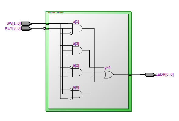
The file mux4x1.v descibes a very simple multiplexer circuit where the inputs are provided with the pushbuttons SW0-SW3 and the channel selector are the switches SW0-SW1 in binary. The output is displayed on the the first red LED (LEDR0).
Wikipedia provides the following diagram:

Quartus synthesises an equavalent circuit shown below:
Although a multiplexer is not used in the calculator, the thought of making a calculator occured to me at this point in the journey. I decided to make a calculator first and not a full-fledged general-purpose computer because for the computer, instructions were redily available.
Now we inch closer to making the calculator by displaying decimal numbers from 0-255 based on the input provided on SW0-SW3. I started with displaying the output of 4 bits to one of the seven-segment-displays (HEX0) available on the DE1. The file bin2ssd.v is listed as follows:
module bin2ssd #(
        parameter INVERT = 1'b0
    )(
        input wire[3:0] b,
        output wire[6:0] s
    );

    wire[6:0] seg;
    assign seg =(b == 4'h0) ? 7'b0111111 :
                    (b == 4'h1) ? 7'b0000110 :
                    (b == 4'h2) ? 7'b1011011 :
                    (b == 4'h3) ? 7'b1001111 :
                    (b == 4'h4) ? 7'b1100110 :
                    (b == 4'h5) ? 7'b1101101 :
                    (b == 4'h6) ? 7'b1111101 :
                    (b == 4'h7) ? 7'b0000111 :
                    (b == 4'h8) ? 7'b1111111 :
                    (b == 4'h9) ? 7'b1101111 :
                    (b == 4'hA) ? 7'b1110111 :
                    (b == 4'hB) ? 7'b1111100 :
                    (b == 4'hC) ? 7'b0111001 :
                    (b == 4'hD) ? 7'b1011110 :
                    (b == 4'hE) ? 7'b1111001 :
                                  7'b1110001 ;

    assign s = INVERT ? seg ^ 7'b1111111 : seg;


endmodule
As you see, it is simple code that turns on certain segments given certain hex values provided in 4 bits. The parameter INVERT is used to initialize the module specifying that the segements are on when the HEX[6:0] are set low. Thus I negate the values before assigning them to the output in our case. Although the calculator is not to feature a hex display, hex digits were added for completion.
Double dabble - I always knew BCD (binary-coded decimal) representation of binary numbers existed but I never knew what it is used for. While faced with the challenge of displaying decimal numbers, I understood the significance of this method. I came across the most amazing high-quality explanation of the double-dabble technique made by Sebastian Lague. I highly recommend watching it entirely. You should also check out his brilliant Digital Logic Sim Project.
Coming from a programming background, it was facinating to learn how complex combinational logic circuits can be created for purposes that I assumed can only be done with sequential logic. I use parts of the methods demonstrated in the video even further in the calculator project.
The file dabble.v defines the conditionl adder module as described in the video. The top-level module in rig.v implements the double-dabble technique with the same naming conventions as Sebastian’s so it should be self-explanatory when read after watching the video. The listing is below:
module rig
    (
        input wire[7:0] SW,
        input wire[2:0] KEY,
        output wire[6:0] HEX0, HEX1, HEX2, HEX3,
        output wire[9:0] LEDR,
        output wire[3:0] LEDG
    );

    wire[3:0] doT, doU, doV, doW, doX, doY, doZ;

    dabble dT (.i(SW[7:5]), .o(doT));
    dabble dU (.i({doT[2:0], SW[4]}), .o(doU));
    dabble dV (.i({doU[2:0], SW[3]}), .o(doV));

    dabble dW (.i({doT[3], doU[3], doV[3]}), .o(doW));
    dabble dX (.i({doV[2:0], SW[2]}), .o(doX));

    dabble dY (.i({doW[2:0], doX[3]}), .o(doY));
    dabble dZ (.i({doX[2:0], SW[1]}), .o(doZ));

    assign LEDR[0] = SW[0];
    assign LEDR[4:1] = doZ[3:0];
    assign LEDR[8:5] = doY[3:0];
    assign LEDR[9] = doW[3];

    wire[2:0] k = ~KEY;

    assign LEDG =   (k == 3'h1) ? doT :
                        (k == 3'h2) ? doU :
                        (k == 3'h3) ? doV :
                        (k == 3'h4) ? doW :
                        (k == 3'h5) ? doX :
                        (k == 3'h6) ? doY :
                        (k == 3'h7) ? doZ :
                                          3'h0;

    wire[0:3] bcd1s, bcd10s, bcd100s;

    assign bcd1s = {doZ[2:0], SW[0]};
    assign bcd10s = {doY[2:0], doZ[3]};
    assign bcd100s = {doW[3], doY[3]};

    bin2ssd #(.INVERT(1)) bs0 (.b(bcd1s), .s(HEX0));
    bin2ssd #(.INVERT(1)) bs1 (.b(bcd10s), .s(HEX1));
    bin2ssd #(.INVERT(1)) bs2 (.b(bcd100s), .s(HEX2));

    assign HEX3 = 7'b1111111;

endmoduleWieh my new-found knowledge of 2-s compliment numbers and decimal displays, I decided to make a 10-bit calculator with the 10th bit representing the sign. Thus I had to increase the double-dabble top-level module created above to 9-bits. This modification provided me an opportunity to grasp the double-dabble method more firmly. I also created the reverse of the double-dabble to convert the BCD representation generated after double-dabbling back into binary and displaying it on the red LEDs (LEDR[0]-LEDR[8]). Note that this does not handle 2-s compliement and that will be added in the actual calculator project.
In this listing, I have added a conditional subtractor cond_sub.v which is just an inverse of the conditional adder mentioned earlier. Most of the other listing is the same except the addition of circuitry for one more bit.
wire[3:0] so_a, so_b, so_c, so_d, so_e, so_f, so_g, so_h, so_i;
assign LEDR[0] = bcd1s[0];
cond_sub cs_i (.i({bcd10s[0], bcd1s[3:1]}), .o(so_i));
cond_sub cs_h (.i({bcd100s[0], bcd10s[3:1]}), .o(so_h));
assign LEDR[1] = so_i[0];
cond_sub cs_g (.i({so_h[0], so_i[3:1]}), .o(so_g));
assign LEDR[2] = so_g[0];
cond_sub cs_f (.i({bcd100s[1], so_h[3:1]}), .o(so_f));
cond_sub cs_e (.i({so_f[0], so_g[3:1]}), .o(so_e));
assign LEDR[3] = so_e[0];
cond_sub cs_d (.i({bcd100s[2], so_f[3:1]}), .o(so_d));
cond_sub cs_c (.i({so_d[0], so_e[3:1]}), .o(so_c));
assign LEDR[4] = so_c[0];
cond_sub cs_b (.i({so_d[1], so_c[3:1]}), .o(so_b));
assign LEDR[5] = so_b[0];
cond_sub cs_a (.i({so_d[2], so_b[3:1]}), .o(so_a));
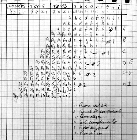
assign LEDR[8:6] = {so_a[2:0]};I made the below rough sheet to aid in coding for the 10-bit double-dabble and it’s inverse.
It was time to try my hand on a bit of sequential logic. The easiest example I found to run was a simple LED blinker. This ‘Hello World!’ of a sequential logic FPGA circuit gave me enough of a start to attempt the calculator next. The file blink.v is listed below.
module rig (
        input  wire CLOCK_50,
        output wire [0:1] LEDR
    );

    blink b0 (
        .clk (CLOCK_50),
        .led (LEDR[0])
    );

     assign LEDR[1] = CLOCK_50;

endmodule

module blink(
        input wire clk,
        output reg led
    );

    reg [31:0] count = 0;

    always @(posedge clk) begin

        if (count == 32'd49_999_999) begin
            count <= 0;
            led <= ~led;
        end else begin
            count <= count +1;
        end

    end

endmodule
Here I use the 50MHz clock of the DE1 as an input and the always block is set to trigger at the positive-edge of the clock and it will only trigger once on each positive-edge. I am counting to 50 million and inverting the current state of the LED. Note that Verilog HDL will compile the addition operation into an adder.
One point to note here is that <= means that the assignment must be done at the end of the clock cycle.
With the fundamentals in place, I was now ready to put it all to practice with the calculator. Was I in for a surprise! It turned out to be one of the most interesting project I implemented.
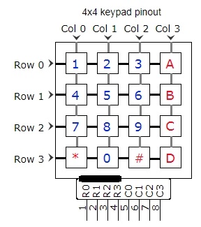
I started with trying to get a 4x4 keypad grid to work. I attached the keypad below to GPIOs on the board.
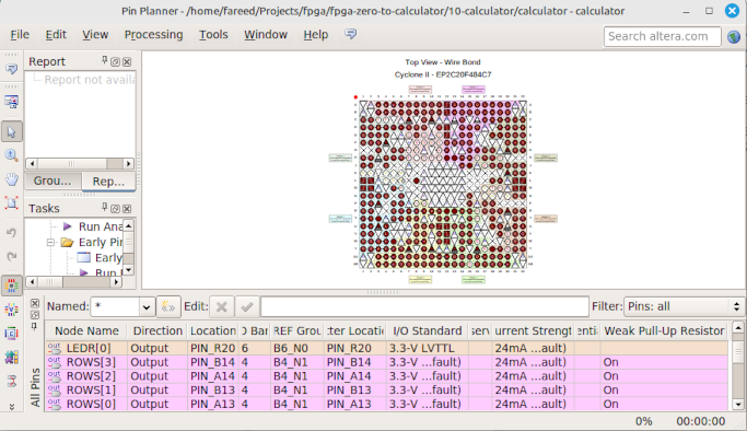
After various failed attempts and much debugging with a multimeter, I got the keypad partially working. I realized that it was required to explicitly specify the pin nodes to have a weak pull-up resistor to avoid them to be in a floating state. This is done through the Pin Editor utility of Quartas as below:
The module in keypad.v takes an input of columns to sense keys while sets rows as otuput. It also outputs ‘pressed’ which goes low when a key is released and it triggers ‘released’ for one clock cycle. The digits that were detected are output as BCD and 4 opers can be output based on the key that was pressed. The listing of keypad.v is as follows:
module keypad
(
input wire clk,
output reg[3:0] rows,
input wire[3:0] cols,
output reg pressed,
output reg released,
output reg[3:0] digits,
output reg[3:0] opers
);
reg[1:0] state = 0;
reg[31:0] count = 0;
reg[2:0] scan_row = 0;
reg[0:0] detected = 0;
initial begin
pressed <= 0;
released <= 0;
digits <= 0;
opers <= 0;
state <= 0;
count <= 0;
detected <= 0;
end
always @(posedge clk) begin
if (count == 0) begin
count <= 32'd49_999; // Sample at 1Khz
case (state)
0: begin
if (scan_row == 4) begin
state <= 2;
scan_row <= 0;
end else begin
state <= 1;
released <= 0;
case (scan_row)
0: rows <= 4'b1110;
1: rows <= 4'b1101;
2: rows <= 4'b1011;
3: rows <= 4'b0111;
default: rows <= 4'b1111;
endcase
end
count <= 0;
end
1: begin
scan_row <= scan_row + 1;
state <= 0;
case (scan_row)
0: begin
if (~cols[0]) begin digits <= 4'd1; detected <= 1; end
else if (~cols[1]) begin digits <= 4'd2; detected <= 1; end
else if (~cols[2]) begin digits <= 4'd3; detected <= 1; end
else if (~cols[3]) begin opers <= 3'd1; detected <= 1; end
end
1: begin
if (~cols[0]) begin digits <= 4'd4; detected <= 1; end
else if (~cols[1]) begin digits <= 4'd5; detected <= 1; end
else if (~cols[2]) begin digits <= 4'd6; detected <= 1; end
else if (~cols[3]) begin opers <= 3'd2; detected <= 1; end
end
2: begin
if (~cols[0]) begin digits <= 4'd7; detected <= 1; end
else if (~cols[1]) begin digits <= 4'd8; detected <= 1; end
else if (~cols[2]) begin digits <= 4'd9; detected <= 1; end
else if (~cols[3]) begin opers <= 3'd3; detected <= 1; end
end
3: begin
if (~cols[1]) begin digits <= 4'd0; detected <= 1; end
else if (~cols[3]) begin opers <= 3'd4; detected <= 1; end
else if (~cols[0]) begin opers <= 3'd5; detected <= 1; end
else if (~cols[2]) begin opers <= 3'd6; detected <= 1; end
end
endcase
end
2: begin
if (detected) begin
pressed <= 1;
detected <= 0;
state <= 0;
end else begin
if (pressed) begin
released <= 1;
state <= 3;
pressed <= 0;
end else state <= 0;
end
count <= 0;
end
3: begin
released <= 0;
digits <= 0;
opers <= 0;
state <= 0;
count <= 0;
end
endcase
end else begin
count <= count - 1;
end
end
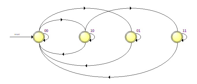
endmoduleAs you can see, I had to ultimately implement it as a state machine with the following states:
Impressively, Quartas sees the state machine and shows this diagram in the state machine viewer:
This is a simpler module than keypad with a small state-machine used to debounce inputs from 4 keys on the DE1. The module pushbtn.v takes the clock and button to debounce as inputs and triggers ‘pressed’ and ‘released’ for one clock cycle. It does so by counting 7 continuous and consistent presses or releases.
In dec2bin.v, the BCD values of each decimal place digit is converted into it’s binary form using this module. This happens continously. Note that there is an input for negative here which when high, produces a 2-s compliment binary number of the BCD digits. The rest of the listing is the same reverse double-dabble as discussed in project 9 encapsulated as a reusable module. Note that I use SystemVerilog HDL here to make 2-dimensional array handling easier.
The bin2dec.sv module is used to convert the outcome of a calculation to decimal numbers to display on the seven-segment display at the instant of evaluation. If the number represented by the 2-s compliment binary input is a negative number, we invert the number and add 1 using combinational logic. We don’t output if the input binary number is negative because if it is, it is easy to find that from the most-significant binary digit. The other parts are similar to the double-dabble as discussed in projects 8 and 9.
The file bin2ssd.v is modified substiantially from the binary to SSD module used in earlier project. I have added comments to each of the input and output wires listed below:
        input wire[3:0] b, // bcd in
        input wire bi, // ripple blanking
        output wire[6:0] s, // ssd
        output wire bo, // ripple blanking output
        input wire mi, // display minus
        input wire rz, // if right digit is zero, don't display minus here
        output wire zo, // is this digit zero? (used by left digit)
        output wire mo // ripple minus if not consumed to avoid negative sign instead of 0 in middle of number
Here I use the ripple blanking concept described in Sebastian Lague’s video posted above. I add another semi-ripple minus segment that is displayed on the next left digit’s g-segment.
It is best to describe the calculator.sv block-by-block.
module calculator
    (
        output wire[3:0] ROWS,
        input wire[3:0] COLS,
        output wire[9:0] LEDR,
        output wire[7:0] LEDG,
        output wire[6:0] HEX0, HEX1, HEX2, HEX3,
        input wire[3:0] KEY,
        input wire CLOCK_50
    );
The following are the inputs and outputs and a description of functionality:
Next we declare the nodes we will be using. I have commented each wire or reg.
    wire[3:0] dec_curr_digit, curr_oper;    // Outputs of keypad module
    wire[3:0] result_dec[2:0];              // Result of computation
    reg[3:0] dec_digits[2:0],               // Current displayed value in BCD
                dec_curr_digit_latched = 0, // New digit latched while shifting left
                curr_oper_latched= 0;       // Operator latched when second operand entered
    wire dec_digits_negative;               // Is the dec_digits negative
    reg[2:0] dec_idx = 0,                   // Index of input cursor
                shift_iter;                 // Used for shifting left
    reg[9:0] operand1, result;              // The 1st operand and result of calculation in binary
    reg[0:0] disp_result;                   // Next cycle will display 'result' on dec_digits
    wire released;                          // Released trigger from keypad module
    reg[3:0] key_rel;                       // Push button's (KEYs) debounced released trigger
Next we wire up the keypad:
    keypad kp (
        .digits(dec_curr_digit),
        .opers(curr_oper),
        .pressed(LEDG[7]),
        .released(released),
        .rows(ROWS[3:0]),
        .cols(COLS[3:0]),
        .clk(CLOCK_50)
    );
The below loop is not a loop like a programming loop. It can be thought of like a template to generate hardware resources instead of writing HDL repeatedly. Here we use the pushbtn module for debouncing.
    // Iterate generation of four debounced pushbtns
    genvar i;
    generate
        for (i = 0; i < 4; i = i + 1) begin: btn_gen
            pushbtn #(.INVERT(1)) btn(.clk(CLOCK_50), .button(KEY[i]), .released(key_rel[i]));
        end
    endgenerate
Following are the combinational circuits that are stateless continuous:
    wire rbo;
    wire[2:0] z;    // If left digit is 0
    wire[1:0] m;    // Ripple display negative sign

    bin2ssd #(.INVERT(1)) bs3 (.b(), .mi(dec_digits_negative), .s(HEX3), .bi(1), .rz(z[2]), .mo(m[1]));     // use this only for negative sign
    bin2ssd #(.INVERT(1)) bs2 (.b(dec_digits[2]), .mi(m[1]), .s(HEX2), .bi(1), .bo(rbo), .rz(z[1]), .zo(z[2]), .mo(m[0]));
    bin2ssd #(.INVERT(1)) bs1 (.b(dec_digits[1]), .mi(m[0]), .s(HEX1), .bi(rbo), .rz(z[0]), .zo(z[1]));
    bin2ssd #(.INVERT(1)) bs0 (.b(dec_digits[0]), .s(HEX0), .bi(0), .zo(z[0]));

    // The dec_digits are converted to binary and stored in LEDR ready for operations
    dec2bin db (.bcds(dec_digits), .negative(dec_digits_negative), .bin2c(LEDR));

    // result is kept ready in bcd form to set into the dec_digits when disp_result is high on a clock positive-edge
    bin2dec bd (.bcds(result_dec), .bin2c(result));
We initialize 4 BCD to seven-segment-display converters. There are some complications to display the negative sign on the leftmost non-zero digit but not the first digit but if you follow the ripple concept explanained in Sebastian’s videos, the code should be intutive. I have commented the rest of the code and it should be self explanatory.
The numbers are input as follows:
end else if (released) begin // If keypad key was released
            // Below checks if applicable digit was pressed (as no curr_oper was pressed)
            if (!curr_oper && ((dec_idx == 0 && dec_curr_digit != 0) || dec_idx == 1 || dec_idx == 2)) begin
                if (dec_idx == 0 && curr_oper_latched) begin // first digit after oper button pressed
                    dec_digits[0] <= 0;
                    dec_digits[1] <= 0;
                    dec_digits[2] <= 0;
                    dec_digits_negative <= 0;
                end

                dec_curr_digit_latched <= dec_curr_digit;
                shift_iter <= dec_idx + 1;
In the above, the first part is the state just when a number is entered subsequent to an oper key being pressed. On each clock cycle, when a number is pressed, we shift the existing digits left for which we run shift_iter from the current index to 1 as below.
// If shifting in progress
        if (shift_iter) begin
            if (shift_iter == 1) begin // On the last shift iter
                // Set the last digit to the latched
                dec_digits[0] <= dec_curr_digit_latched;
                dec_idx <= dec_idx + 1;
                shift_iter <= 0;
            end else begin // Shift a digit left
                dec_digits[shift_iter - 1] <= dec_digits[shift_iter - 2];
                shift_iter <= shift_iter - 1;
            end
        end else if (disp_result) begin
            // If computation was done and result has to be displayed
            dec_digits[0] <= result_dec[0];
            dec_digits[1] <= result_dec[1];
            dec_digits[2] <= result_dec[2];
            dec_digits_negative <= result[9];
            disp_result <= 0;
        end
If an oper(ation) key is pressed,
end else if (curr_oper) begin // An oper key was pressed
                if (curr_oper == 3'd6) begin    // Negate number
                    dec_digits_negative <= !dec_digits_negative;
                end else begin // All other operations
                    curr_oper_latched <= curr_oper;
                    dec_idx <= 0;
                    operand1 <= LEDR;
                end
            end // curr_oper
We latch the operation and store the current binary value as operand1.
When = is pressed, we evaluate the result and set the result to be displayed on the next clock cycle.
if (key_rel[0]) begin   // = key pressed
            if (curr_oper_latched == 3'd1) begin
                result <= operand1 + LEDR;
                disp_result <= 1; // result will be displayed on the next clock
            end else if (curr_oper_latched == 3'd2) begin
                result <= operand1 - LEDR;
                disp_result <= 1;
            end if (curr_oper_latched == 3'd3) begin
                result <= operand1 * LEDR;
                disp_result <= 1;
            end else if (curr_oper_latched == 3'd4) begin
                result <= operand1 / LEDR;
                disp_result <= 1;
            end
This is how the result is displayed on the next clock cycle:
        end else if (disp_result) begin
            // If computation was done and result has to be displayed
            dec_digits[0] <= result_dec[0];
            dec_digits[1] <= result_dec[1];
            dec_digits[2] <= result_dec[2];
            dec_digits_negative <= result[9];
            disp_result <= 0;
        end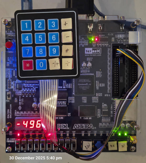
I’m hoping to soon scale up this project to an 8-decimal-digit calculator with fixed decimal point so stay tuned.
And that’s all folks!